Silicon to silicon nitride interlayer transition
A photonic chip guides light in waveguides: strips of a material with a high refractive index, the number that says how strongly a material slows light, set in glass. Silicon nitride, with a lower index than silicon, loses less light and carries more power. A chip with a nitride layer above its silicon gets both, and a second level where guides cross without touching, but the light must move between the layers. It travels as a mode, a field pattern that keeps its shape; TE0, the simplest, has its electric field across the strip. The silicon and nitride modes travel at different speeds, so an abrupt step reflects and scatters light. An interlayer transition overlaps two opposed tapers: the silicon narrows until its mode spills upward, while the nitride above widens to catch it. When the change is slow, the mode follows and changes guide with little loss. The figure of merit is the insertion loss, the power that fails to arrive, in decibels (dB), a logarithmic scale on which 0.1 dB is about 2 %; good transitions lose 0.1 to 0.5 dB over 50 nm or more.
This notebook builds the transition of Huang et al., Opt. Express 22, 21859 (2014) at its lowest-loss overlap, 50 µm, and reads the TE0 insertion loss across 1530 to 1600 nm: 0.084 dB at 1550 nm, against the paper's stated 3D FDTD bound of 0.25 dB and measured bound of 0.2 dB.
Parameters
The design numbers are the paper's; the guide widths are assumed, and the library's silicon nitride stands in for its deposited film. The band is the paper's measured spectrum. The mesh is uniform, since the taper walls cross the cells at a very shallow angle. The sideways clearance holds six decay lengths of the nitride mode's tail. A mirror plane at y = 0 halves the run.
# design, the paper's Sec. 2
h_si = 0.22  # silicon guide thickness (µm)
g = 0.10  # oxide between silicon and nitride (µm)
h_sin = 0.60  # nitride guide thickness (µm)
w_tip_si = 0.20  # silicon taper tip (µm)
w_tip_sin = 0.30  # nitride taper tip (µm)
L = 50.0  # taper length, both layers (µm)
Lo = 50.0  # overlap of the two tapers (µm)
w_si = 0.50  # assumed: silicon guide width (µm)
w_sin = 1.00  # assumed: nitride guide width (µm)
nitride = ph.materials.Si3N4  # assumed: n 2.00; 1.90 adds 0.24 dB at Lo=10
paper_il_sim_db = 0.25  # paper, stated 3D FDTD bound, Lo > 20 µm (dB)
paper_il_meas_db = 0.2  # paper, stated measured bound, Lo = 50 µm (dB)
# simulation choices
wlen_min = 1.53  # band start (µm)
wlen_max = 1.60  # band end (µm)
n_wlen = 15  # wavelengths read out
cells_per_wlen = 18  # mesh cells per wavelength in silicon
lead = 4.0  # straight guide before each port (µm)
clearance = 1.3  # nitride edge to PML, sideways (µm)
clearance_z = 1.0  # guides to PML, above and below (µm)
pml = 16  # PML layers
symmetry = (0, -1, 0)  # mirror normal to y
transits = 6  # longest run, in transits of the device
shutoff = 1e-5  # field decay that ends the run

wlen = np.linspace(wlen_min, wlen_max, n_wlen)  # wavelengths (µm)
wlen0 = 1.55  # wavelength of the headline number (µm)
f0 = ph.c0 / (wlen0 * 1e-6)  # its frequency (Hz)
Geometry
Each guide is a ph.Polygon, an outline in the chip plane (vertices_um, an
edge and its mirror image) extruded through its layer (slab_bounds_um);
ph.Structure gives it a medium. The nitride sits g above the silicon's top
at z = 0. The silicon narrows over L; the nitride widens over L, starting
Lo before the silicon tip. A straight lead carries each guide to its port.
The function draws both at any overlap, for the sweep.
def transition(Lo):
    """The silicon and nitride tapers at overlap `Lo`, centred on x = 0."""
    x_si = -(2 * L - Lo) / 2  # where the silicon taper starts (µm)
    x_sin = (2 * L - Lo) / 2  # where the nitride taper ends (µm)
    edge_si = [(x_si - lead, w_si / 2), (x_si, w_si / 2), (x_si + L, w_tip_si / 2)]
    edge_sin = [(x_sin - L, w_tip_sin / 2), (x_sin, w_sin / 2), (x_sin + lead, w_sin / 2)]
    outline_si = [(x, -y) for x, y in edge_si] + edge_si[::-1]  # counter-clockwise
    outline_sin = [(x, -y) for x, y in edge_sin] + edge_sin[::-1]
    return [
        ph.Structure(
            geometry=ph.Polygon(axis="z", vertices_um=outline_si, slab_bounds_um=(-h_si, 0.0)),
            medium=ph.materials.Si,
        ),
        ph.Structure(
            geometry=ph.Polygon(axis="z", vertices_um=outline_sin, slab_bounds_um=(g, g + h_sin)),
            medium=nitride,
        ),
    ]


structures = transition(Lo)
Simulation
A ph.Port is a plane across a guide: its centre, the axis the light travels
along, and the guide's width and thickness. TE0 is launched at in on the
silicon and read at out on the nitride, so light left in the silicon or
scattered does not count. ph.mode_window_um sizes the window each mode is
solved and read in, at the longest wavelength: 20 % beyond where its intensity
falls 30 dB below the peak. That margin would take the wide nitride mode's
window into the absorbing layer (PML) above, so its window stops at the 30 dB
line (factor=1.0).
window_si = ph.mode_window_um(w_si, h_si, ph.materials.Si, ph.materials.SiO2, wlen_max)
window_sin = ph.mode_window_um(w_sin, h_sin, nitride, ph.materials.SiO2, wlen_max, factor=1.0)


def ports_at(Lo):
    """The silicon input and the nitride output at overlap `Lo`."""
    reach = (2 * L - Lo) / 2 + lead  # centre to each port plane (µm)
    return [
        ph.Port("in", (-reach, 0.0, -h_si / 2), "x", w_si, thickness_um=h_si, window_um=window_si),
        ph.Port(
            "out", (reach, 0.0, g + h_sin / 2), "x", w_sin, thickness_um=h_sin, window_um=window_sin
        ),
    ]


ports = ports_at(Lo)
ph.Simulation holds the setup. ph.Domain fits the box around the
structures with the clearances and continues each guide through the PML;
ph.Mesh sets cells_per_wlen cells per wavelength in silicon, the same
everywhere. The field monitor records the side view through both guides at
1550 nm; the auto-shutoff ends the run once the light has left.
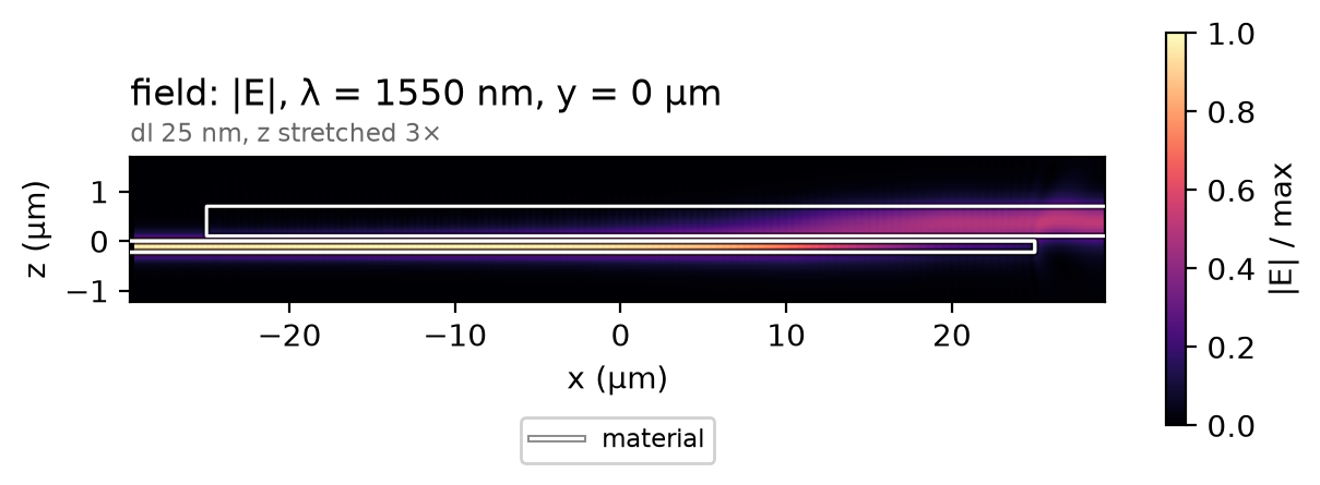
field = ph.ProfileMonitor.plane("field", "y", 0.0, wlens_um=wlen0)  # side view, guides' axis
sim = ph.Simulation(
    domain=ph.Domain(clearance_um=(clearance, clearance, clearance_z)),
    mesh=ph.Mesh(cells_per_wlen=cells_per_wlen, uniform=True),
    background=ph.materials.SiO2,  # oxide cladding
    pml_num_layers=pml,
    structures=structures,
    symmetry=symmetry,
    wlens_um=wlen,  # wavelengths read out at the ports
    ports=ports,
    source="in",  # the port that launches TE0
    run=ph.RunSpec(transits=transits, shutoff=shutoff),
    monitors=[field],
)
sim.plot_index(y=0.0)
plt.show()
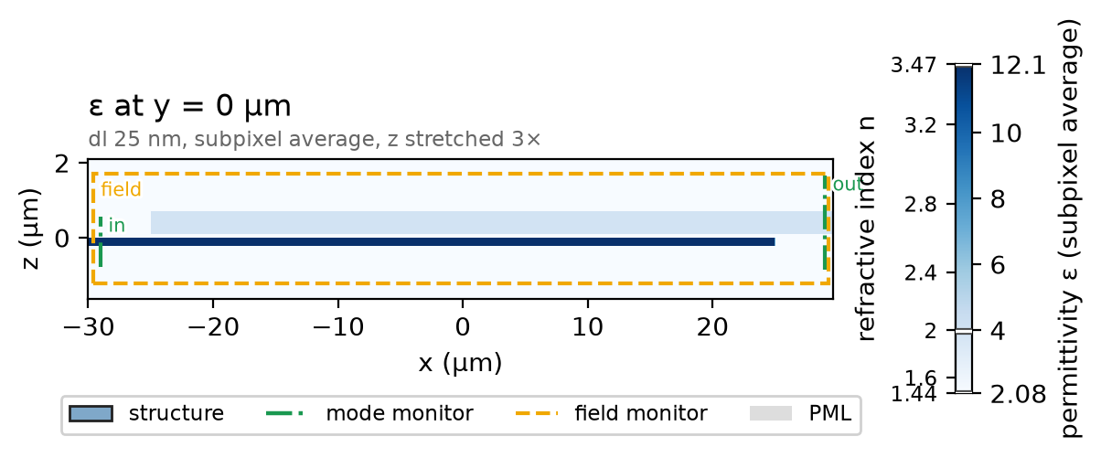
ph.run_local runs the solver on this computer; ph.cloud.run_quoted runs it
on a cloud GPU. The outputs on this page come from a GPU run of this exact
simulation.
data = ph.run_local(sim, quiet=True)
# On a cloud GPU instead, with GPU and SOLVER from your closed-test guide:
# data = ph.cloud.run_quoted(sim, device=GPU, solver=SOLVER)
Field
The light stays in the silicon while the silicon is wide, spreads upward through the oxide as the silicon narrows beneath the widening nitride, and is carried by the nitride well before the silicon tip at x = 25 µm.
Result
The insertion loss is −10 log₁₀ of the nitride's TE0 power at out over the
TE0 power launched in the silicon. The dashed lines are the paper's stated
bounds; the article's licence does not allow re-plotting its curves here.
T = data.transmission("out")  # nitride TE0 over the launched silicon TE0
il_db = -10 * np.log10(T)  # insertion loss (dB)
ph.viz.plot_comparison(
    il_db,
    stated=[
        (paper_il_sim_db, "paper, stated (3D FDTD bound, Lo > 20 µm)"),
        (paper_il_meas_db, "paper, stated (measured bound, Lo = 50 µm)"),
    ],
    ylabel="insertion loss (dB)",
    ylim=(0.0, 0.4),
)
plt.show()
il_1550 = float(il_db.sel(f=f0, method="nearest"))
print(f"insertion loss at 1550 nm: {il_1550:.3f} dB")
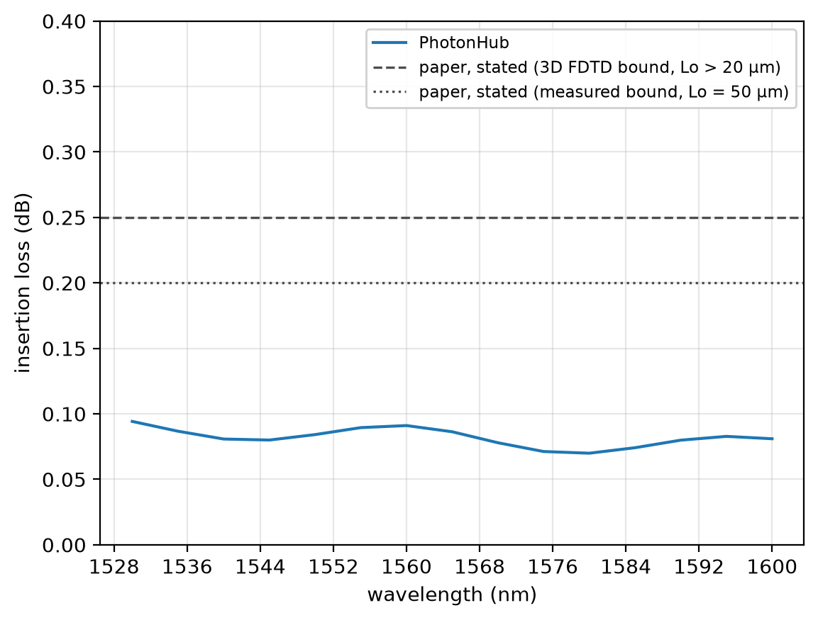
At 18 cells per wavelength the insertion loss reads 0.084 dB at 1550 nm; at 30 cells, 0.091 dB, not shown converged; the paper's 3D FDTD, below 0.25 dB for every overlap longer than 20 µm. The run uses a uniform mesh of 18 cells per wavelength in silicon, subpixel averaging on, non-dispersive silicon, nitride and oxide, 16 PML layers and one mirror plane normal to y.
Sweep
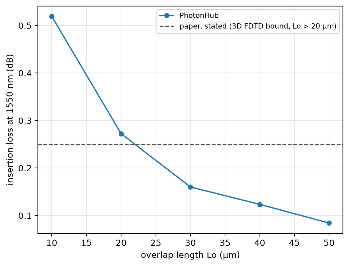
The paper's own sweep, at this mesh: the same device at overlaps from 10 µm to 50 µm, each a full run. The loss falls as the tapers share more length and the handover becomes gradual; the paper finds it below 0.25 dB beyond 20 µm.
overlaps = [10.0, 20.0, 30.0, 40.0]  # the paper's sweep, below Lo (µm)
sweep_db = []
for lo in overlaps:
    sim_lo = sim.with_changes(structures=transition(lo), ports=ports_at(lo))
    T_lo = ph.run_local(sim_lo, quiet=True).transmission("out")
    sweep_db.append(-10 * np.log10(float(T_lo.sel(f=f0, method="nearest"))))
all_lo = [*overlaps, Lo]  # every overlap, with the run above (µm)
all_db = [*sweep_db, il_1550]  # loss at 1550 nm (dB)
ph.viz.plot_comparison(
    np.array(all_lo),
    np.array(all_db),
    stated=(paper_il_sim_db, "paper, stated (3D FDTD bound, Lo > 20 µm)"),
    xlabel="overlap length Lo (µm)",
    ylabel="insertion loss at 1550 nm (dB)",
)
plt.show()
print(" | ".join(f"{lo:.0f} µm: {v:.3f} dB" for lo, v in zip(all_lo, all_db)))