Polarization rotator-splitter in a foundry stack
Light reaches a chip from an optical fibre, which carries two polarizations, two orientations of the electric field, in a mix that drifts with time. A silicon waveguide, a strip of silicon in glass that guides light, treats them very differently, so most circuits handle one. Light travels along it as modes, field patterns that keep their shape: TE0, the simplest, has its electric field across the strip, TM0 has it upright. A polarization rotator-splitter passes TE0 straight on and turns TM0 into TE0 on a second waveguide, so the rest of the chip sees one polarization on two paths. A plain strip cannot turn TM0, because it is mirror symmetric top to bottom. A thinner, partly etched slab beside the strip breaks that symmetry: along a slow taper TM0 becomes TE1, the two-lobed TE mode, and a long coupler hands TE1 to a second strip as its TE0. The figures of merit are in decibels (dB), a logarithmic scale on which 1 dB is about 21 %: the conversion loss, typically under 1 dB, and the crosstalk, the power in the wrong output, typically under −15 dB.
This notebook builds the all-adiabatic device of Sacher, Barwicz, Taylor and Poon, Opt. Express 22, 3777 (2014) from its Fig. 1(a) and reads the TM₀ to TE₀ transmission across 1500 to 1580 nm: −0.131 dB at 1540 nm, against the fabricated device's stated loss under 1.5 dB. Every crosstalk term stays under −26 dB, against the measured −13 dB.
Parameters
The design numbers are the paper's Fig. 1(a); the arc's turn, the straightening bend and the broad arm's output taper are assumed. The band is the paper's measurement window. The mesh is uniform, the same cell in silicon and oxide: a graded mesh with coarse oxide cells reads this device low. The leads are six mode widths; the clearances hold four decay lengths of the TM₀ tail.
# design, the paper's Fig. 1(a)
h = 0.22  # silicon thickness (µm)
h_slab = 0.09  # slab (µm): use your foundry's partial-etch depth
w_in = 0.45  # input strip width (µm)
w_mid = 0.55  # ridge width at the taper midpoint (µm)
w_slab = 1.55  # slab width at the taper midpoint (µm)
w_wide = 0.85  # ridge width at the taper end (µm)
L_taper = 100.0  # bi-level taper, two equal halves (µm)
w_broad_end = 0.65  # broad arm width at the coupler end (µm)
w_tip = 0.20  # narrow arm tip at the coupler start (µm)
w_narrow = 0.50  # narrow arm width at the coupler end (µm)
gap = 0.20  # coupler gap (µm)
L_coupler = 300.0  # adiabatic coupler length (µm)
R_arc = 450.0  # radius of the arc leading the narrow arm away (µm)
w_out = 0.50  # output waveguide width (µm)
theta = 6.0  # assumed: turn of that arc (degrees)
R_back = 100.0  # assumed: radius of the arc straightening it (µm)
L_out_taper = 30.0  # assumed: broad arm's taper to w_out (µm)
paper_il_db = 1.5  # paper, Sec. 2.2: measured loss bound (dB)
paper_xt_db = -13.0  # paper, Sec. 2.2: measured crosstalk bound (dB)
paper_band = (1.53, 1.58)  # paper, Sec. 2.2: band of both bounds (µm)
# simulation choices
wlen_min = 1.50  # band start (µm)
wlen_max = 1.58  # band end (µm)
n_wlen = 17  # wavelengths read out
cells_per_wlen = 9  # in silicon (49 nm); keep the mesh uniform
lead = 3.0  # straight guide before each port (µm)
clearance = 1.0  # silicon edge to PML, beside the device (µm)
clearance_z = 1.0  # core to PML, above and below (µm)
pml = 12  # PML layers
transits = 3  # longest run, in transits of the device
shutoff = 1e-5  # field decay that ends the run

wlen = np.linspace(wlen_min, wlen_max, n_wlen)  # wavelengths (µm)
wlen0 = 0.5 * (wlen_min + wlen_max)  # band centre (µm)
f0 = ph.c0 / (wlen0 * 1e-6)  # band-centre frequency (Hz)
Geometry
The taper starts at x = 0, the broad arm runs along y = 0 and the core is
centred on z = 0. Each straight part is a ph.Polygon, an outline in the chip
plane (vertices_um, an upper edge and its mirror image) extruded through its
layer (slab_bounds_um). The slab widens to w_slab at the taper midpoint
and closes again; the full-height ridge runs through the taper, becomes the
coupler's broad arm and narrows to w_out. The narrow arm starts as a tip one
gap away.
x1 = L_taper / 2  # taper midpoint (µm)
x2 = L_taper  # coupler start (µm)
x3 = L_taper + L_coupler  # coupler end (µm)
th = np.radians(theta)  # turn of the arcs (rad)
x_out = x3 + (R_arc + R_back) * np.sin(th) + lead  # output port planes (µm)
z0 = -h / 2  # core bottom (µm)
slab_edge = [(0.0, w_in / 2), (x1, w_slab / 2), (x2, w_wide / 2)]
ridge_x = [-lead, 0.0, x1, x2, x3, x3 + L_out_taper, x_out]
ridge_w = [w_in, w_in, w_mid, w_wide, w_broad_end, w_out, w_out]
ridge_edge = [(x, w / 2) for x, w in zip(ridge_x, ridge_w)]
slab = ph.Polygon(
    axis="z",
    vertices_um=[(x, -y) for x, y in slab_edge] + slab_edge[::-1],
    slab_bounds_um=(z0, z0 + h_slab),
)
ridge = ph.Polygon(
    axis="z",
    vertices_um=[(x, -y) for x, y in ridge_edge] + ridge_edge[::-1],
    slab_bounds_um=(z0, z0 + h),
)
narrow = ph.Polygon(
    axis="z",
    vertices_um=[
        (x2, -w_wide / 2 - gap - w_tip),
        (x3, -w_broad_end / 2 - gap - w_narrow),
        (x3, -w_broad_end / 2 - gap),
        (x2, -w_wide / 2 - gap),
    ],
    slab_bounds_um=(z0, z0 + h),
)
The narrow arm leaves on the arc of radius R_arc, and a second arc
straightens it. Each arc is a ph.Cylinder sector: outer and inner radii one
guide width apart, between two angles. A ph.Box carries the arm on to its
port, and ph.Structure gives every shape the library's silicon.
y3 = -(w_broad_end / 2 + gap + w_narrow / 2)  # narrow arm's axis, coupler end (µm)
x4 = x3 + R_arc * np.sin(th)  # where the two arcs meet (µm)
y4 = y3 - R_arc * (1 - np.cos(th))
y5 = y3 - (R_arc + R_back) * (1 - np.cos(th))  # narrow arm's axis at its port (µm)
bend_away = ph.Cylinder(
    axis="z",
    center_um=(x3, y3 - R_arc, 0.0),
    radius_um=R_arc + w_out / 2,
    inner_radius_um=R_arc - w_out / 2,
    length_um=h,
    angle_start_rad=np.pi / 2 - th,
    angle_stop_rad=np.pi / 2,
)
bend_back = ph.Cylinder(
    axis="z",
    center_um=(x4 + R_back * np.sin(th), y4 + R_back * np.cos(th), 0.0),
    radius_um=R_back + w_out / 2,
    inner_radius_um=R_back - w_out / 2,
    length_um=h,
    angle_start_rad=-np.pi / 2 - th,
    angle_stop_rad=-np.pi / 2,
)
out_lead = ph.Box(center_um=(x_out - lead / 2, y5, 0.0), size_um=(lead, w_out, h))
shapes = [slab, ridge, narrow, bend_away, bend_back, out_lead]
structures = [ph.Structure(geometry=s, medium=ph.materials.Si) for s in shapes]
Simulation
A ph.Port is a plane across a guide: its centre, the axis the light travels
along, the guide's width and thickness, and the mode it launches or reads.
TM₀ enters at in. The broad arm's output reads TE₀ and TM₀ (through,
through_tm: the TE branch), the narrow arm's output TE₀ (cross, the wanted
signal) and TM₀ (cross_tm). ph.mode_window_um sizes each window at the
longest wavelength, 20 % beyond where the mode's intensity falls 30 dB below
its peak. TM₀ reaches further into the oxide: that margin would take its
window into the absorbing layer (PML), so the TM₀ windows stop at the 30 dB
line (factor=1.0).
window_in = ph.mode_window_um(
    w_in, h, ph.materials.Si, ph.materials.SiO2, wlen_max, mode="TM0", factor=1.0
)
window_tm = ph.mode_window_um(
    w_out, h, ph.materials.Si, ph.materials.SiO2, wlen_max, mode="TM0", factor=1.0
)
window_te = ph.mode_window_um(w_out, h, ph.materials.Si, ph.materials.SiO2, wlen_max, mode="TE0")
ports = [
    ph.Port("in", (-lead, 0.0, 0.0), "x", w_in, thickness_um=h, mode="TM0", window_um=window_in),
    ph.Port("through", (x_out, 0.0, 0.0), "x", w_out, thickness_um=h, window_um=window_te),
    ph.Port(
        "through_tm", (x_out, 0.0, 0.0), "x", w_out, thickness_um=h, mode="TM0", window_um=window_tm
    ),
    ph.Port("cross", (x_out, y5, 0.0), "x", w_out, thickness_um=h, window_um=window_te),
    ph.Port(
        "cross_tm", (x_out, y5, 0.0), "x", w_out, thickness_um=h, mode="TM0", window_um=window_tm
    ),
]
ph.Simulation holds the setup. ph.Domain fits the box around the device
with the clearances and continues every guide through the PML; ph.Mesh sets
cells_per_wlen cells per wavelength in silicon, the same everywhere. The
field monitor records the core plane at the band centre.
field = ph.ProfileMonitor.plane("field", "z", 0.0, wlens_um=wlen0)  # the core mid-plane
sim = ph.Simulation(
    domain=ph.Domain(clearance_um=(clearance, clearance, clearance_z)),
    mesh=ph.Mesh(cells_per_wlen=cells_per_wlen, uniform=True),
    background=ph.materials.SiO2,  # oxide cladding
    pml_num_layers=pml,
    structures=structures,
    wlens_um=wlen,  # wavelengths read out at the ports
    ports=ports,
    source="in",  # the port that launches TM0
    run=ph.RunSpec(transits=transits, shutoff=shutoff),
    monitors=[field],
)
sim.plot_index(z=0.0)
plt.show()
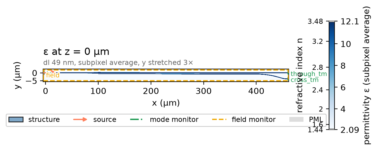
ph.run_local runs the solver on this computer; ph.cloud.run_quoted runs it
on a cloud GPU. The outputs on this page come from a GPU run of this exact
simulation.
data = ph.run_local(sim, quiet=True)
# On a cloud GPU instead, with GPU and SOLVER from your closed-test guide:
# data = ph.cloud.run_quoted(sim, device=GPU, solver=SOLVER)
Field
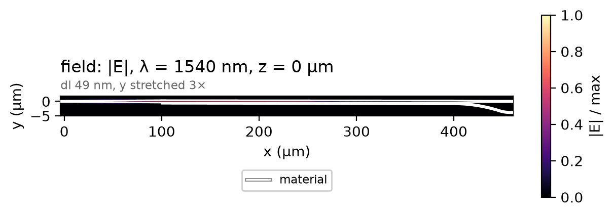
The single-lobed TM₀ becomes the two-lobed TE₁ in the first half of the taper, rides the broad arm, drains into the narrow arm well inside the coupler and leaves on the arc as TE₀; almost nothing reaches the TE branch.
Result
The observable is the TM₀ to TE₀ transmission at the TM branch, modal power over launched modal power, in dB. The dashed line is the paper's stated loss bound for the fabricated device; the article's licence does not allow re-plotting its measured curves here. The crosstalk is the largest of what reaches the TE branch and the TM₀ left at the TM branch.
T = data.transmission("cross")  # TM0 in, TE0 out at the TM branch
T_db = 10 * np.log10(T)
leak = np.maximum(data.transmission("through"), data.transmission("through_tm"))
xt_db = 10 * np.log10(np.maximum(leak, data.transmission("cross_tm")))  # largest leak (dB)
ph.viz.plot_comparison(
    T_db,
    stated=(-paper_il_db, "paper, stated (measured loss bound, 1530-1580 nm)"),
    ylabel="TM₀ in, TE₀ out at the TM branch (dB)",
    ylim=(-2.0, 0.5),
)
plt.show()
in_band = (T.wlen_um.round(4) >= paper_band[0]) & (T.wlen_um.round(4) <= paper_band[1])
xt_worst = float(xt_db.where(in_band).max())  # worst crosstalk in the paper's band (dB)
T_1540 = float(T_db.sel(f=f0, method="nearest"))
print(
    f"TM0 -> TE0 at 1540 nm: {T_1540:+.3f} dB | worst crosstalk over 1530-1580 nm: "
    f"{xt_worst:.1f} dB (paper: under {paper_xt_db:.0f} dB)"
)
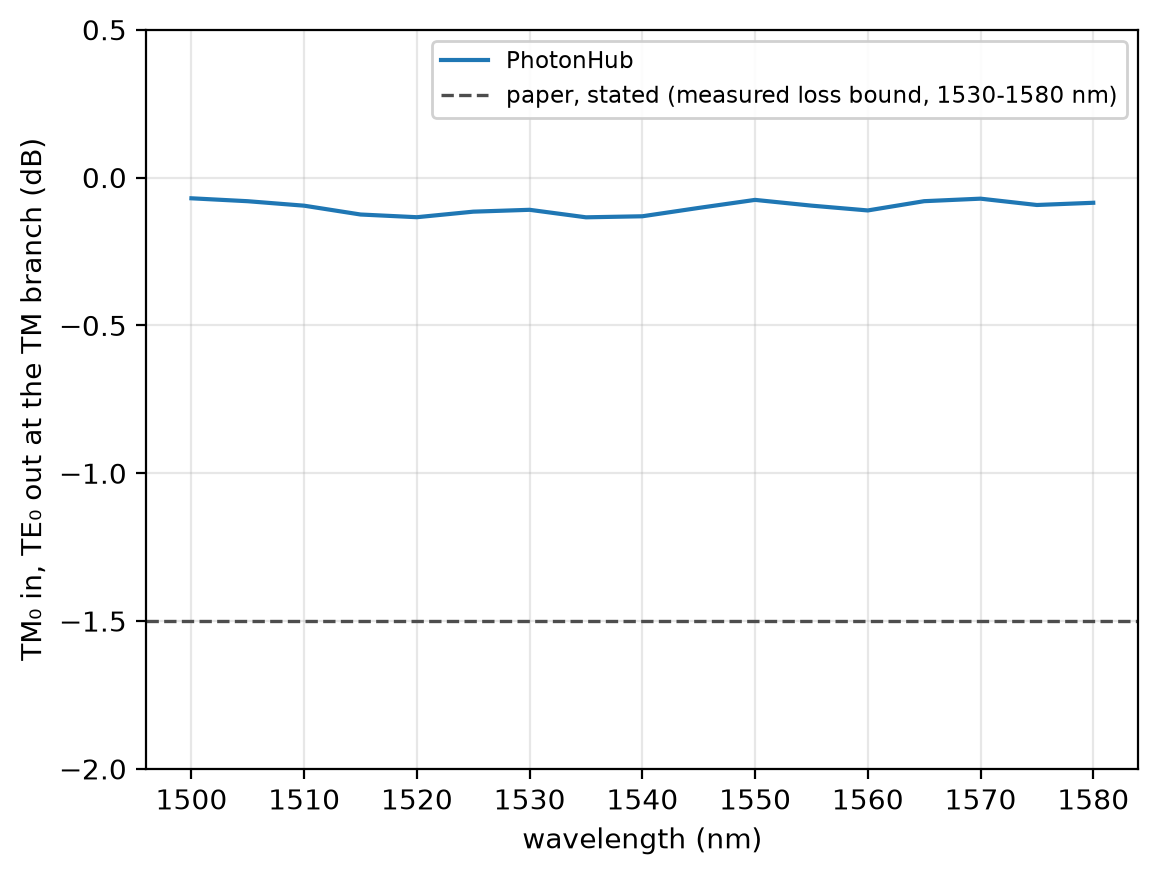
TM0 -> TE0 at 1540 nm: -0.131 dB | worst crosstalk over 1530-1580 nm: -27.0 dB (paper: under -13 dB)
At 9 cells per wavelength the TM₀ to TE₀ transmission reads −0.131 dB at 1540 nm; at 11 cells, −0.058 dB at 40 nm, not shown converged; the paper's measured device, within −1.5 dB. The run uses a uniform 49 nm mesh, subpixel averaging on, non-dispersive silicon and oxide, 12 PML layers and no symmetry plane.